Search
2017 Kyoto Prize Laureates
Electronics
/ Semiconductor Engineer
1944 -
Honorary Fellow, Fujitsu Laboratories Ltd. / Executive Visiting Researcher, Advanced ICT Research Institute, National Institute of Information and Communications Technology
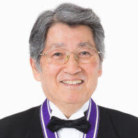
My Fifty Years with Transistor
2017
11 /11 Sat
Place:Kyoto International Conference Center
History of the Development of Compound Semiconductor Electronic Devices and Its Future Possibilities
2017
11 /12 Sun
13:00 - 17:10
Place:Kyoto International Conference Center
Dr. Mimura invented the High Electron Mobility Transistor (HEMT) with a new structure, in which two layered semiconductors are stacked. He revealed that HEMT has excellent high-frequency characteristics because of its high mobility nature of electrons. This invention has led to significant advancements both in information and communications technology and in physics studies of electrons confined in ultrathin conductive layers.
In 1979, Dr. Mimura invented a new transistor, called High Electron Mobility Transistor (HEMT) by stacking two semiconductors of different electron affinities. He noticed that if a semiconductor with smaller electron affinity is placed on a semiconductor having a larger affinity and is doped with positive impurities, highly-mobile electrons would be formed along the interface of these two semiconductors. He demonstrated the first transistor operation of the HEMT by controlling the concentration of electrons with a voltage applied to its gate. He then showed that, because of the high-mobility of electrons, the HEMT excelled in its high- frequency characteristics. He played leading roles in the development of HEMTs as micro- wave and millimeter-wave devices by exploring their applications to radio astronomy and broadcasting satellite (BS) systems. Thus, he contributed immensely to the progress of information and communications technology. Moreover, as electrons in the HEMT move only in two dimensions (2D) along the interface with nearly no influence of impurities, the HEMT has served as an ideal system for the study of physics of electrons with reduced dimensions.
About a decade before the HEMT invention, Esaki and Tsu devised a novel concept of a superlattice (SL), in which two different ultrathin semiconductors were alternately stacked. Promoted by this work, SLs consisting of GaAs and AlGaAs were formed and studied to show the 2D nature of electron in GaAs layers. It was also discovered in 1978 that if such SLs were formed by introducing positively impurities only into AlGaAs layers, all the electrons would be confined in GaAs layers and show high mobility, as they were separated from impurities. Inspired by this work, Dr. Mimura realized that, if a single AlGaAs layer, containing positive impurities is deposited onto a GaAs layer, it would induce high-mobility electrons along the AlGaAs/GaAs interface, which led eventually to the HEMT invention.
Because of superior high-frequency characteristics, HEMTs are widely used in such areas as receivers for BS systems, base stations in mobile phone systems, and millimeter-wave car-borne radars; thus, HEMTs serve as one of indispensable high-speed devices, by which the information and communications technology is built. Although HEMTs were fabricated first by the combined use of AlGaAs and GaAs, the choice of materials was expanded to the InAlAs/InGaAs pair and other systems. Recently, AlGaN/GaN HEMTs have been developed and widely used as high-frequency power devices for base stations of mobile phone systems; this system is getting to be used also as high-voltage power-controlling devices.
As stated above, the invention of HEMTs by Dr. Mimura and a set of his subsequent works have made outstanding contributions to the progress of information and communications technology and also to the remarkable advancement in physics studies of low-dimensional electrons.
For these reasons, the Inamori Foundation is pleased to present the 2017 Kyoto Prize in Advanced Technology to Dr. Takashi Mimura.
Profile is at the time of the award.
"Being of Service" Means to Be Needed and Appreciatedby the Overwhelming Majority
In the second installment of the series “Unearthing the Words of Kyoto Prize Laureates,” we were privileged to interview Dr. Takashi Mimura, the 2017 Kyoto Prize laureate in the Advanced Technology category.

Dr. Mimura turned “Honorable Doctor,” Kwansei Gakuin University
On December 7, 2017, the presentation ceremony was held at Kwansei Gakuin University (here in after KG) ; the “Honorable Doctor” was given to Dr. Mimura, for his great achievements of research as well as the 2017 Kyoto Prize awarded in November.