Search
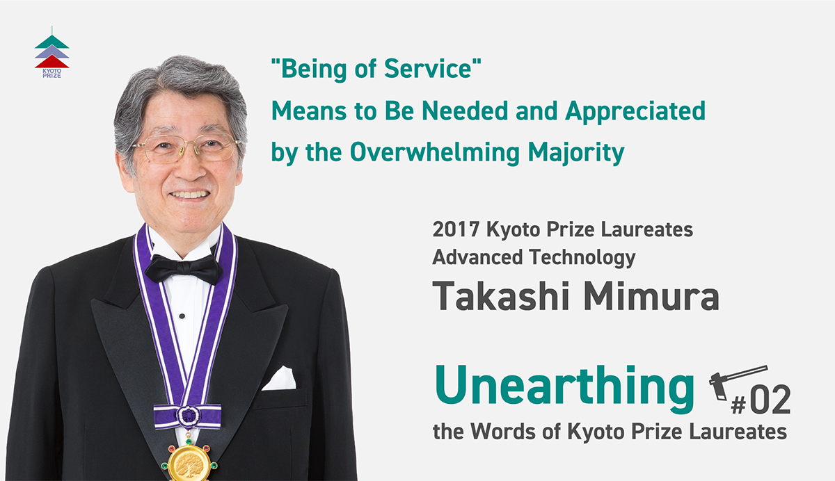
An international award of Japanese origin, the Kyoto Prize is presented to individuals who have made significant contributions in the fields of science and technology, as well as arts and philosophy. Kyoto Prize laureates are those who have made an extra effort to plumb the depths of their chosen fields and profoundly inspired the scientific, cultural, and spiritual betterment of humankind through their achievements. In this series of “Unearthing the Words of Kyoto Prize Laureates,” we will interview the past laureates of the Kyoto Prize and take a closer look at the words that they delivered at their Commemorative Lectures to get to the heart of their unique ideas, thought process, and attitudes as inquirers. In the second installment of the series, we were privileged to interview Dr. Takashi Mimura, the 2017 Kyoto Prize laureate in the Advanced Technology category.
Previous article in “Unearthing the Words of Kyoto Prize Laureates”
#1 Dr. Toyoki KunitakeYou’re Sure to Find a Breakthrough in the Process of Going Back and Forth Between “Abstraction” and “Materialization”
──────────────
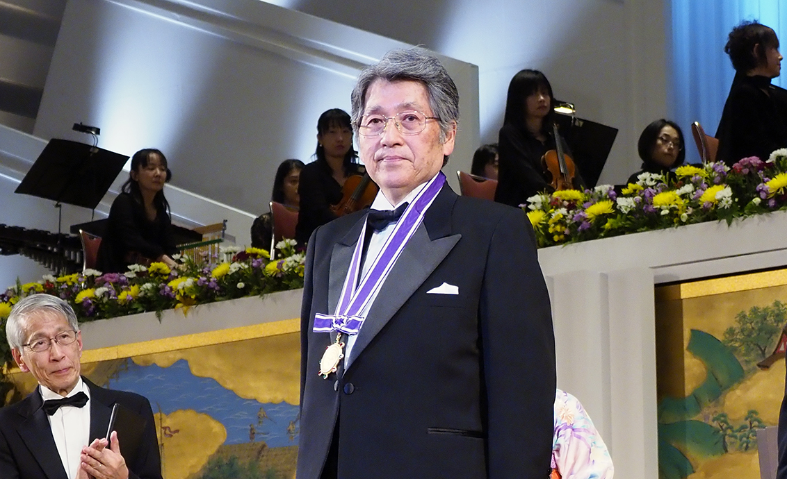
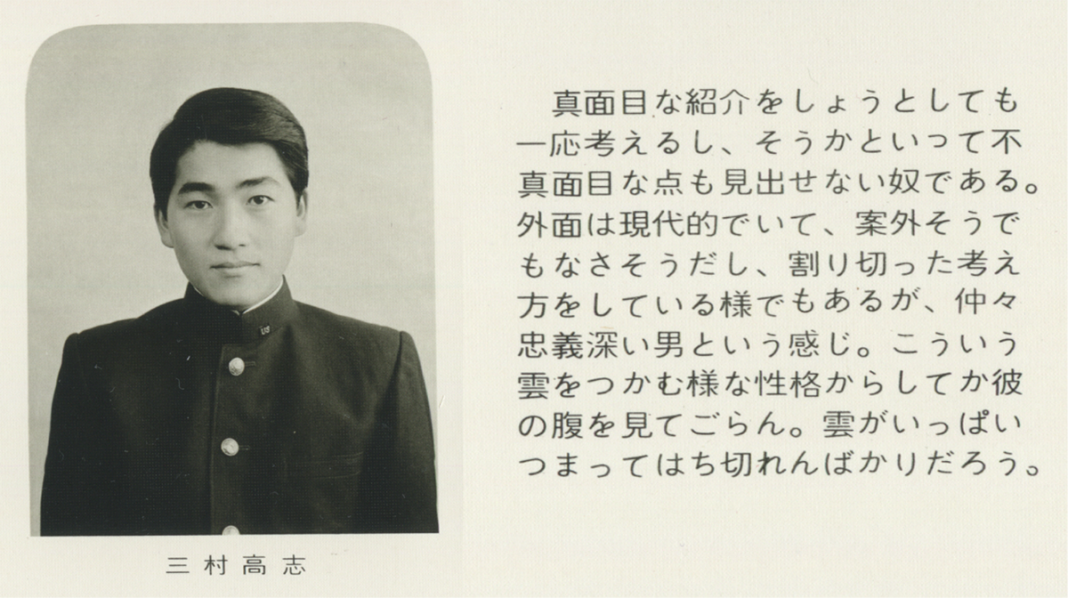
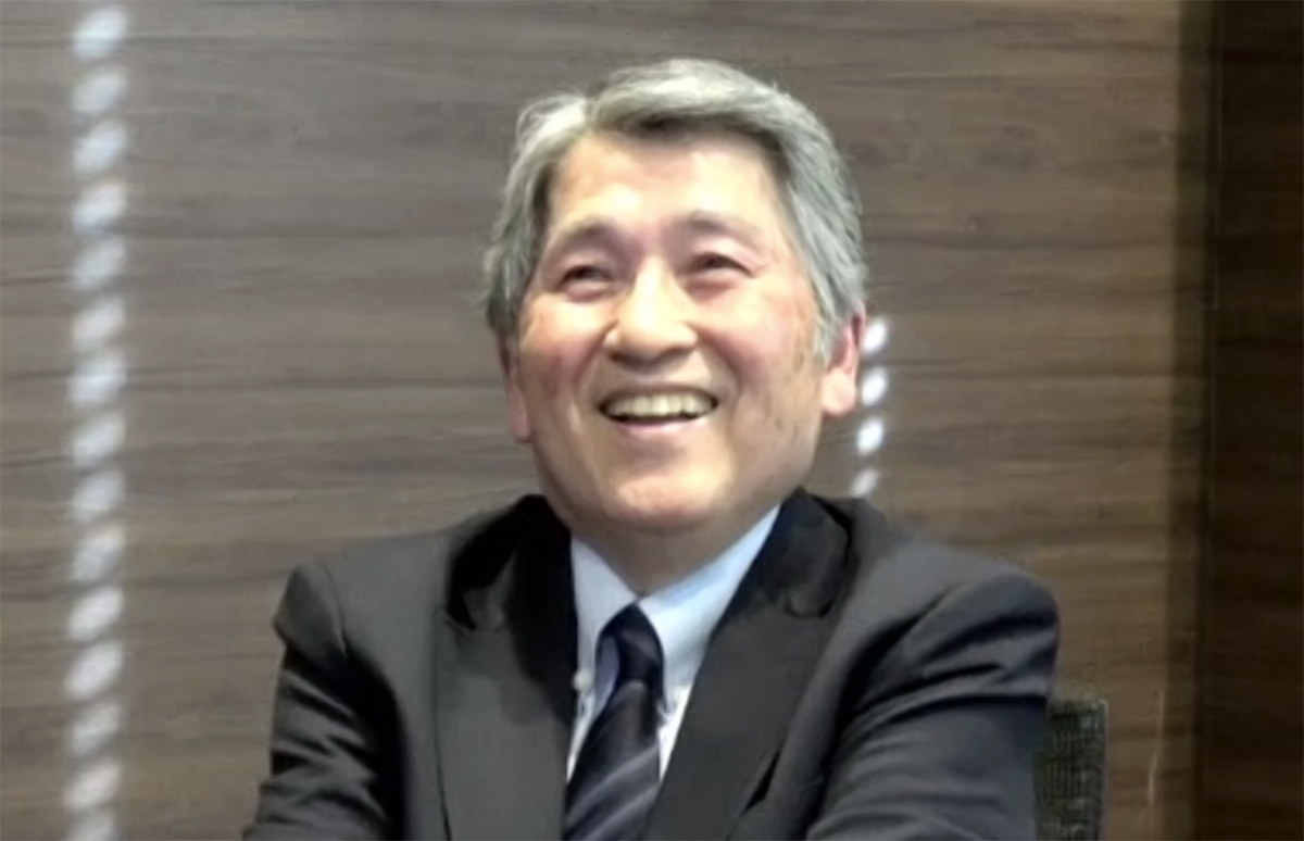
Takashi Mimura
Honorary Fellow, Fujitsu Ltd., and Executive Visiting Researcher, Advanced ICT Research Institute, National Institute of Information and Communications Technology (NICT). After receiving a Master’s degree in Engineering from the Graduate School of Engineering Science, Osaka University, Mimura joined Fujitsu Ltd. in 1970 and was transferred to Fujitsu Laboratories, Ltd. in 1975. He earned his Ph.D. in Engineering from Osaka University in 1982 and was appointed Honorary Fellow, Fujitsu Laboratories Ltd. in 2017. Read more
Nishimura May I start by asking you to give us a brief description of your research?
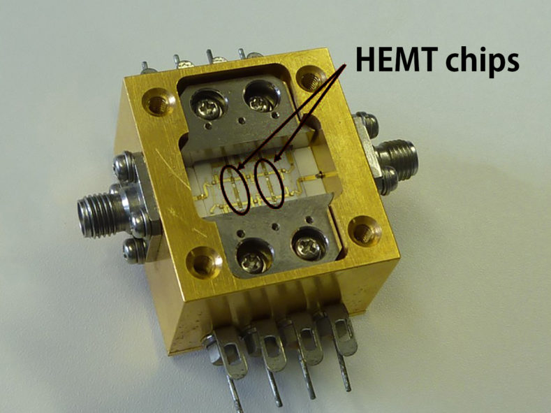
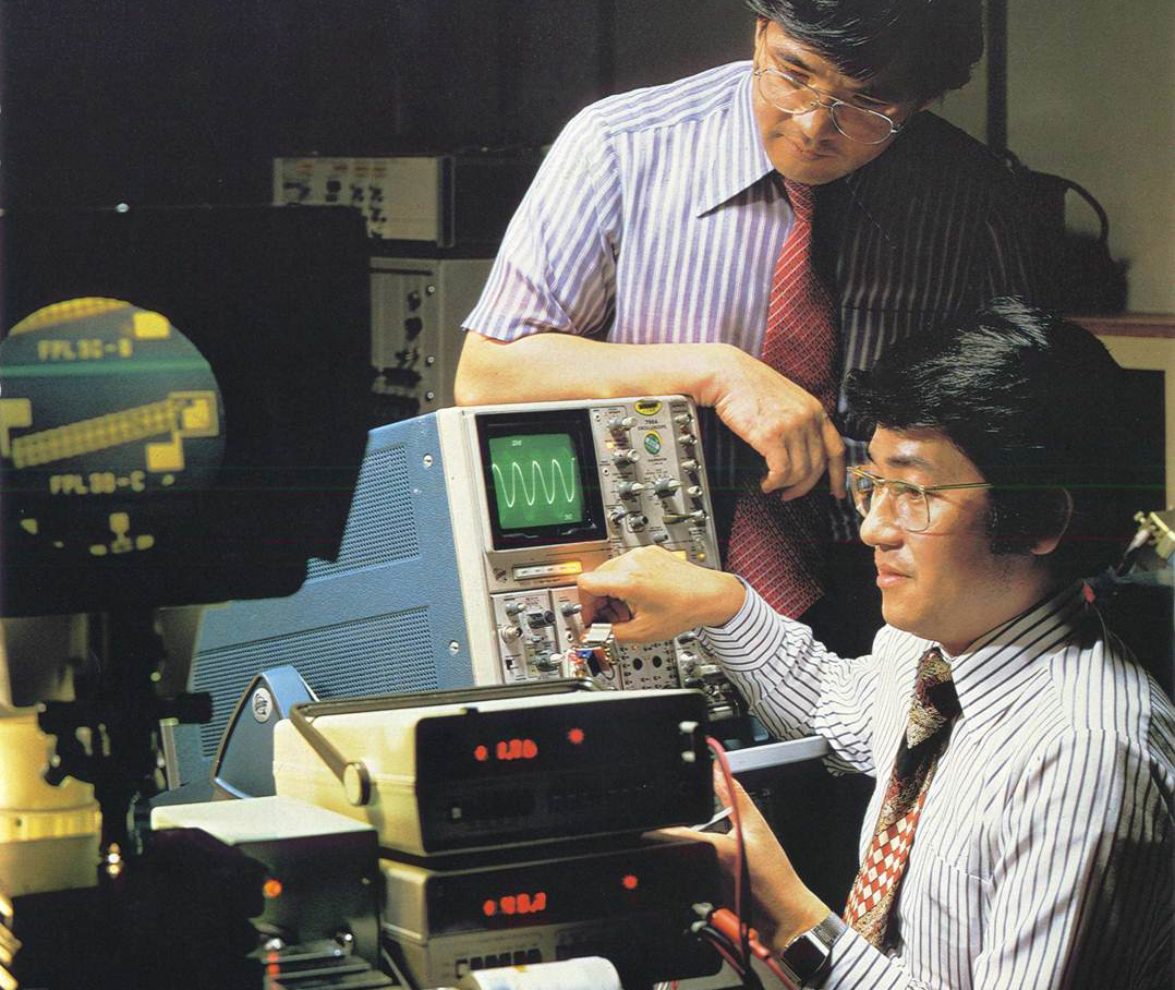
Mimura I received the Kyoto Prize in recognition of my invention of the high electron mobility transistor (HEMT).*1 The HEMT excels in its high-frequency and high-speed characteristics, because of higher mobility of electrons*2 than conventional transistors. But I didn’t intend to invent a HEMT from the beginning. The truth is that I came up with the idea of a HEMT after trying many different kinds of devices.
Nishimura I hear that you studied optical properties at Osaka University but, when you joined Fujitsu, you were assigned to a very unexpected post and so began working on transistors.
Mimura At Osaka University, I was at Dr. Shin’ichiro Narita’s lab, making germanium with a high-impurity concentration to study its far-infrared optical properties. You could say it was truly basic research. I joined Fujitsu because Dr. Narita was working at Kobe Industries Corp. at the time (later merged with Fujitsu). I believe Dr. Narita thought I would be assigned to a team working on optical properties, but some complication sent me to their transistor section.
A transistor is an electronic component used to amplify or switch electronic signals and comprises a p-type semiconductor with positive property and an n-type semiconductor with negative property. By changing the potential distribution of holes and electrons, which serve as carriers when forming a p-n junction,*3 it functions the way you want it to. At Fujitsu, I got to know a thing called an electronic device for the first time, and I became intrigued by the fact that it has its own functions.
Soon after that, I got a call from someone asking me to join the optical property team, but I asked them to let me continue working on devices, as I had already become taken with p-n junctions.
Nishimura Since you specialized in basic research at the Graduate School of Engineering Science, I assume that at one time you had an interest in basic research. But you found yourself very intrigued by applied research, didn’t you?
Mimura I guess so. Transistors were invented in 1948, and I joined Fujitsu in 1970. It was a time when there were still a lot of research projects that took very dynamic approaches. In fact, research on transistors and optical properties had one thing in common—“Studying responses to external stimulus.” In the case of optical property research, you shed light on objects to see what will happen. The difference was that devices offer practical benefits, which was enormously appealing to me.
Nishimura The very beginning of the process leading up to the invention of the HEMT was a technical challenge of developing high-speed transistors, right?
Mimura If we could increase the speed of transistors, we could process a large amount of information in a short time and transmit and receive high-frequency radio signals. It was predicted that information and telecommunication systems of various kinds would make a quantum leap if that became a reality. Now, to make transistors work faster, you need to increase electron mobility as much as possible. Back in the 1970s, much attention was paid to GaAs MESFETs (Metal-Semiconductor Field Effect Transistors), which use gallium arsenide (GaAs), a compound semiconductor whose mobility is about five times higher than that of silicon.
But it had long been assumed that GaAs MESFETs were the ultimate high-speed devices and that all that device developers could do would be to modify them. So, in 1977 my team began research into GaAs Metal-Oxide-Semiconductor Field Effect Transistors (GaAs MOSFETs),*4 to seek the possibility of making them faster than silicon MOSFETs (Si MOSFETs), which had already existed. At the time, no researcher had succeeded in creating a GaAs MOSFET that would operate by inducing electrons along the GaAs surface. In this sense, we were truly going where none had gone before.
About a year after we began our research, however, I concluded that we did not stand a chance of accumulating electrons on the surface of GaAs. So I changed my goal and began assessing the switching performance of MOSFETs with a donor doped current path which can function with relatively many surface levels. For the sake of recording how far the development had come, I wrote a paper on our initial attempt. We chose the 37th Device Research Conference, or DRC, in June 1979 as the occasion to read the paper and bring an end to our GaAs MOSFET research for good.
Nishimura In light of having to discontinue your research, I think it was very important that you put together the fruits of what you had so painstakingly worked on to present at the DRC.
Mimura I had worked on the project for about two years, but with no apparent light ahead, I decided to call it a day. Still, I was confident that what we had achieved was among the very best in the world, and I thought it worthwhile to compile an account of “we have come this far.”
GaAs MOSFET research was authorized by Fujitsu Laboratories. To give it up meant that we would have no authorized research topic. You could say that my back was against the wall, and I was half prepared to lose my job. Then, about three weeks after my presentation at the DRC, the idea of the HEMT came to me. It wasn’t like a power born out of a moment of extreme danger, but I guess the bitter experiences of failure somehow sharpened my senses and gave me strength.
Sugimoto How did you get the idea of the HEMT?
Mimura It just struck me when I was chatting with an American researcher at the DRC reception. On the return flight from the U.S., I could not think of anything other than the HEMT. Although I didn’t have a clear idea at that stage, I was somehow convinced that this would work. After three weeks of intensive thinking, I finally arrived at a concrete idea of the HEMT in July 1979.
Nishimura If your GaAs MOSFET research was good enough to write a world-class paper, I think you could safely say that the research had its merits, and so you could have carried on to take a chance with it. Yet, you decided otherwise, but I guess that’s the key to the birth of the next brilliant idea.
Mimura You’re right. Because I gave it up, I had some “space” in me, which led me to my next idea.
Nishimura It astonishes me to learn that you presented a paper on the HEMT at the 38th DRC in the following year. I imagine that you were working with a sense of urgency unique to a lab affiliated with a private business.
Mimura I guess so. You could say that private enterprises are more light-footed and can move more dynamically.
Nishimura I imagine you also had difficulties unique to working in a corporate lab.
Mimura If you’re working at a corporate lab, it’s easier to accelerate your research with focus, but at the same time, they may not allow you to go on with your research on the sole basis of it being innovative. If I may give you an example, liquid crystal displays, or LCDs, were developed in 1968 by an American company called RCA,*5 but the LCDs were put to practical use in the form of electronic calculators from Sharp Japan in 1973. This was due to the lack of understanding on the part of RCA’s display division, because CRT television sets were at their zenith at the time. I shouldn’t generalize, but there are more cases than you may think where an invention from a corporate lab takes longer before it reaches the market than it should because of human barriers.
Nishimura My next question is, how did you manage to hold on to your conviction that you should carry the research out because investigating it was fascinating?
Mimura Well, it takes a group of like-minded people to do so. Important people at business divisions got promoted to where they are because of past technologies. It’s natural that they would hesitate to work on cutting-edge technologies no one ever tried before.
To demonstrate my idea on the HEMT, we needed advanced crystal growth technology called molecular-beam epitaxy,」*6 or MBE. I was lucky enough to have a group of researchers working on MBE then within Fujitsu Laboratories. When I sought their cooperation and told them about my idea for the HEMT, they readily agreed without question.
It seemed they thought the MBE technology they had was too advanced and so they were looking for devices of a level of sophistication that would require their technology. As I briefed them on my idea, I had a feeling in my bones that this was it. In any case, without their cooperation, the HEMT wouldn’t have been released by Fujitsu.
Sugimoto Did you have a plan B in case you didn’t get the cooperation from the MBE group?
Mimura I knew one of my senior researchers was working on MBE outside Fujitsu, and so I could seek help from him. It made me realize how effective the alumni network was.
In my case, it just happened my company had a group that possessed the critical technology and I was able to have their full support. So, we set up a cross-organizational small prototype study circle to start joint research. But then again, this research began as an “unofficial” project that had not been authorized by Fujitsu Laboratories, as we did not explicitly let them know about it. We only had a very limited window of time for this research, but we managed to complete the prototype study in about four months, having gathered experimental data that ended up being used for our very first paper on the HEMT.
Nishimura You invented the HEMT because you were intrigued and attracted to the idea that devices can be “of service.” Could you explain what it means to you to make something that is “of service?”
Mimura If something is “of service,” it is appreciated by people, right? I think the importance of taking action for others that they appreciate is in the DNA of humankind.
Nishimura The invention of the HEMT would come to change the world dramatically. How did you perceive fascinating things that were born because of the HEMT?
Mimura The HEMT made significant contributions to the progress of radio astronomy. Perhaps the most fascinating story is how it was involved in NASA’s Voyager program.*7 Voyager 1 and 2 robotic interstellar probes were launched in 1977, before the HEMT came into existence.

Voyager 2 took images of Jupiter in 1979 and Saturn in 1981, then approached Neptune and Pluto. To capture observational data sent via very weak radio waves, an American radio observatory installed a HEMT amplifier into every antenna. Guess what happened? They got crystal clear images of Neptune and other planets! In Japan, Nobeyama Radio Observatory set up a HEMT amplifier in 1985, which contributed to the discovery of an unknown hydrocarbon molecule in a dark nebula.*8
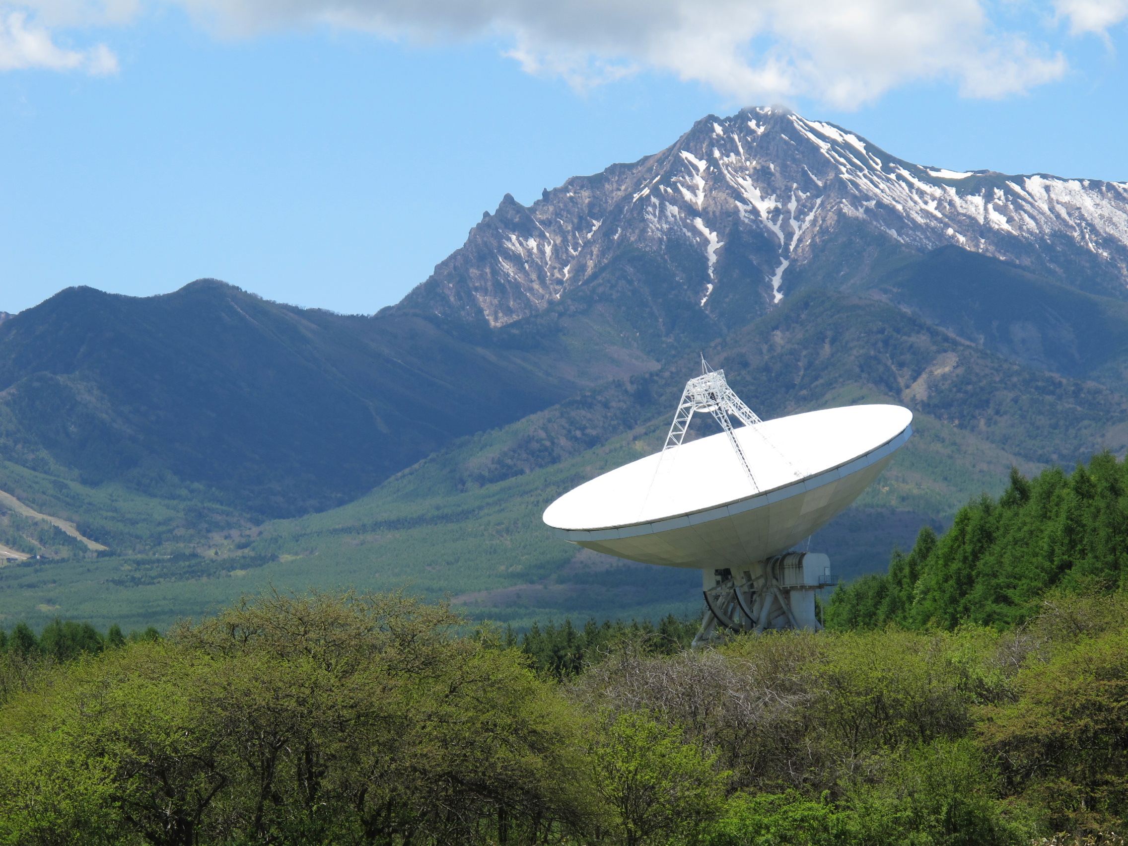
After that, major radio observatories around the world began using a HEMT amplifier. The fact that we were able to find a market where the HEMT’s performance could be harnessed in the initial development stage helped us find yet another area for application as we continued improving the technology.
Nishimura If it were not for the HEMT, the resolution of Voyager’s images of the band of the planet Jupiter would have been a lot lower.
Mimura Or they had to use a gigantic antenna to receive radio signals. The HEMT was also instrumental in downsizing antennas for receiving signals from broadcast satellites. In the midst of the Cold War, continental Europe was divided into the East and the West, and antennas with a built-in HEMT sold like pancakes because Eastern European nations could watch BS channels from the West. I don’t have any good evidence for this, but the birth of the HEMT may have indirectly triggered the fall of the Berlin Wall.
Because the HEMT is the fastest functioning transistor, it has the natural advantage of working where radio waves are sent and received. More recently, it is used in mobile phone base stations. My interpretation of “being of service” is to be needed and appreciated by the overwhelming majority.
Sugimoto Listening to you speak, I was made to realize how much impact your invention of the HEMT has had in recent history. My question is, what feelings did you have as you watched your invention, the HEMT, change the world?
Mimura I’m glad that the HEMT was not something dangerous, but many technologies evolve because of wars, such as nuclear power and computers, the latter of which was used to calculate trajectories of ballistic missiles. Today, I’d love to see technologies that everyone welcomes the evolution of, but I don’t want to develop anything if it’s out in the world.
Nishimura Even if it pleases people when it is invented, there’s always the possibility that the invention could be put to dangerous use once it hits the market.
Mimura That is true, and it’s something we should always pay attention to, because more than a few technologies are dangerous and useful at the same time. I’m afraid it can be very dangerous if they are put to unexpected use. I guess the question of research ethics has arisen in the field of biotechnology as well.
Nishimura In the past, big research projects had to involve a certain number of researchers, but, due to technological progress, there are more and more things that individual researchers can do alone. I think now more than ever, researchers are required to have stringent individual ethics. Now, how and where did you get the value of “say no to dangerous things?”
Mimura I was into making models of rockets in my junior high and high school years. Back then, gunpowder was easily available at drug stores, and so I used to make pencil rockets from cardboards and fly them. But one day, a rocket suddenly exploded, and I lost my hearing for three days or so. Instances like that made me realize that you can’t judge risk before you literally get hurt.
Nishimura It must have been a very impactful experience that has had a lingering effect throughout your life. Today, safety always comes first, but, because of the lack of opportunities to experience imminent danger, some people grow up without learning the latent danger in things.
Mimura That’s right. I guess this is a very difficult topic to deal with.
Nishimura If we look back on some forty years since the invention of the HEMT, we have seen progress in information and telecommunication technology, which pushed the boundaries of outer space that humankind can reach and significantly increased the amount of information that individuals can get, right? It is an instance that brings to light the magnitude of basic technology in that it can change the very foundation of things.
Today, you’ve brought our attention to the critical role of basic technology, that is, without the invention of the HEMT, there wouldn’t be the applied technology of making antennas for radio observatories and BS broadcasts smaller. I also got the impression that it is your discontinued GaAs MOSFET project that led to the invention of the HEMT.
Mimura People often say that ideas are just new combinations of what is already known. In the case of the HEMT, I think I was able to convince myself that an idea with a slightly different direction might work, because I had worked on GaAs MOSFETs.
Nishimura So, if I use an analogy of a map, you’ll get to know the land’s topography if you draw the oceans first. In other words, by understanding each piece, you’ll get to know where you should focus on. To me, it’s like you found new possibilities because you dived into different fields, rather than because you collected materials that you needed in your field, right?
Mimura Exactly. What was important to me was that I could see how the concept of different devices was linked. The key piece of the HEMT concept was modulation-doped superlattices,*9 which I got to know while writing a paper on GaAs MOSFETs. Because I learned about the accumulation of electrons from my experience with GaAs MOSFETs, I was able to spot relevant information related to technologies from different fields.
In fact, many researchers were working with a HEMT then, and numerous technologies similar to mine had been patented. But the crucial last piece was in a different technological field, which made things difficult for other researchers. To come up with new ideas, it is very effective to keep the scope of your research wide, so that you can visit different fields to bring something back to your own.
Nishimura It seems then, that because you always chased something, you were able to broaden your research scope, which in turn provided links among different concepts.
Sugimoto When you work on something, you focus on your research so much, as evidenced by your ability to give the HEMT idea concrete shape within a matter of only three weeks. At the same time, however, I heard that you make it a rule not to do overtime work. Does that mean that you followed a principle of doing your utmost during the regular eight working hours?
Mimura Honestly, working for eight hours was my limit. After all, you could reflect on how your experiments are doing after you return home. I made it a rule to decide what I would be doing first thing the next morning before I went to bed. I simply couldn’t bear to see my work efficiency drop.
Nishimura I think I’ve learned that research work advances as researchers move back and forth between focusing on research and reflecting on it by seeing things in perspective. Thank you very much again, Dr. Mimura.
*1. high electron mobility transistor (HEMT) A transistor using fast-moving electrons that are accumulated on the junction interface (boundary surface) of two kinds of semiconductors. Achieving superior processing speed, HEMTs have found their applications in parabolic antennas, car navigation systems, automotive radar, and mobile phone base stations.
*2. mobility of electrons An indicator of ease of electrons moving within a substance. HEMTs offer high mobility of electrons.
*3. p-n junction A boundary or interface between p-type and n-type semiconductors.
*4. GaAs Metal-Oxide-Semiconductor Field Effect Transistors (GaAs MOSFETs) MOSFETs are field-effect transistors (FETs) with a three-layered metal-oxide-semiconductor structure. Dr. Mimura used gallium arsenide (GaAs) as a base material to create MOSFETs.
*5. RCA Radio Corporation of America. A multinational electronics company in the U.S. Acquired by General Electric Company in 1986.
*6. molecular-beam epitaxy A technique used to grow high-purity, quality crystals as beams of gas molecules evaporated by heating materials reach a substrate of equipment in a vacuum without colliding with other molecules. The film thickness of crystals can be controlled precisely.
*7. Voyager program An exoplanet and extrasolar exploration program by the National Aeronautics and Space Administration (NASA). In 1977, the two unmanned probes, Voyager 1 and 2, were launched. So far, they have observed Jupiter, Saturn, Neptune, Pluto, and their satellites. After leaving the solar system in 2012, Voyager 1 was approximately 22.4 billion kilometers from the Sun as of June 2020, and is the most distant human-made object from Earth.
*8. Nobeyama Radio Observatory set up a HEMT amplifier in 1985 Observations by radio telescopes in the 1980s revealed that various molecules exist in the dark and cold interstellar space. One such molecule is C6H, which was discovered in 1986 with a 45m radio telescope at Nobeyama Radio Observatory.
*9. modulation-doped superlattices Made by alternating ultra-thin layers of two different kinds of semiconductors, which are high-purity GaAs and AlGaAs doped with a small amount of Si (n-type).
Click below to watch the YouTube video of Dr. Mimura’s Commemorative Lecture from 2017.
Previous article in “Unearthing the Words of Kyoto Prize Laureates”
#1 Dr. Toyoki KunitakeYou’re Sure to Find a Breakthrough in the Process of Going Back and Forth Between “Abstraction” and “Materialization”
[About the interviewer]
Yuya Nishimura
Executive Director, MIRATUKU. Earned a Master’s Degree from the Osaka University Graduate School of Human Science. Built a cross-sector -business and -domain innovation platform, supports leading companies (about 30 annually) in creating new businesses, assists launch of R&D projects, designs future visions, and searches for future trends. Other positions include Innovation Designer, Innovation Design Office, RIKEN, Japan, and Specially Appointed Associate Professor, Social Solution Initiative (SSI), Osaka University MIRATUKU website
[About the writer]
Kyoko Sugimoto
Freelance writer. Earned a Master Degree in Media, Journalism & Communication, Graduate School of Letters, Doshisha University. Interviews researchers, business managers, Buddhist monks, urban designers on such topics as asylums, communities, and Buddhism. Authored Kyodaiteki Bunka Jiten: Jiyu to Kaosu no Seitaikei (Kyoto University Cultural Encyclopedia: Ecosystem of Freedom and Chaos), Film Art, Inc. writin’room