Search
2013 Kyoto Prize Laureates
Electronics
/ Electronics Engineer
1932 - 2024
IBM Fellow, Thomas J. Watson Research Center, IBM Corporation
Reflections on Creativity in My Microelectronics Career
2013
11 /11 Mon
Place:Kyoto International Conference Center
Integrated Circuits: 50 Years of Their Evolution and Future Prospects
2013
11 /12 Tue
10:00 - 17:00
Place:Kyoto International Conference Center
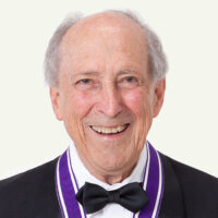
Dr. Robert Heath Dennard invented the basic structure of Dynamic Random Access Memory (DRAM), which is now extensively utilized as one of integrated circuit (IC) memory systems. His innovation has immensely increased the capacity of digital information storage, leading to dramatic progress in information and telecommunications technology. Dr. Dennard and his colleagues also proposed guidelines, called “scaling theory”, to miniaturize field-effect transistors, which play key roles in most ICs, including DRAM, thereby promoting the amazing advance in IC technology.
Dr. Robert Heath Dennard invented the basic structure of the Dynamic Random Access Memory (DRAM) which is now utilized extensively as one of integrated circuit (IC) memory systems. This innovation has immensely increased the capacity of digital information storage, leading to dramatic progress in information and telecommunications technology. Dr. Dennard and his colleagues also proposed design guidelines for miniaturizing MOS (metal oxide semiconductor) field-effect transistors (FETs), which play key roles in most ICs, including DRAM, thereby promoting the amazing advance in IC technology.
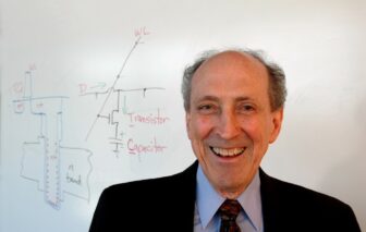
Dr. Dennard began working on memory ICs for computers in the 1960s and invented the basic DRAM structure in 1967. Its fundamental memory unit, or cell, consists of one FET (hereinafter, “transistor”) and one capacitor; each cell stores one bit of data as “1” or “0” by controlling the presence or absence of an electric charge on the capacitor. Cells are arranged on a chip in a matrix form and connected to grid-like wire lines to create a DRAM. The system is called random access memory because it permits any memory cell to be accessed in random order by the selection of a specific horizontal “word” line and a vertical “bit” line, unlike the sequential access memory provided by tape storage.
To store digital information, one bit of data, “1” or “0”, is written in each cell by supplying or removing an electric charge on its capacitor through the transistor. Because the charge thus stored on each capacitor gradually drains away, it is necessary to refresh the capacitor periodically, leading to the name “dynamic” RAM, or DRAM. To read the binary data of a cell, the presence or absence of a stored charge on the capacitor is detected by precisely measuring a change in the electric potential of the bit line.
In 1970, 1k-bit DRAM chip using a three-transistor cell was commercially released, while Dr. Dennard’s one-transistor design made its market debut in 1973. Since then, all the DRAMs have been produced by incorporating the single-transistor structure.
In addition to his DRAM invention, Dr. Dennard and his coworkers studied how FET characteristics changed when they were scaled down, and proposed design guidelines (scaling theory) useful for FET miniaturization. This facilitated the integration of more FETs on a single chip, increasing DRAM storage capacity more than one million-fold, while permitting drastic improvement in the speed and performance of microprocessors and other ICs.
These achievements by Dr. Dennard brought about remarkable developments in integrated circuit technologies, which provided the essential foundation for tremendous progress in information and communications equipments.
For these reasons, the Inamori Foundation is pleased to present the 2013 Kyoto Prize in Advanced Technology to Dr. Robert Heath Dennard.
Profile is at the time of the award.

In Memory of Dr. Dennard, who Has Contributed to the Tremendous Progress in Information and Communications Equipments
The 2013 Kyoto Prize Laureate in Advanced Technology, Dr. Robert Heath Dennard, passed away on April 23, 2024 at the age of 91.
Dr. Robert Dennard Named 2019 Recipient of SIA’s Honor
On June 28, 2019, SIA announced Dr. Robert Dennard has been named the 2019 recipient of SIA’s highest honor, the Robert N. Noyce Award. Dennard will accept the award at the SIA Award Dinner on Nov. 7, 2019 in San Jose. “Dr. Dennard is a semiconductor industry icon, inventing the memory technology underpinning every computer,...